BOM
BOM Cart()
 English
 Russia
 Korean
With its flexible, ultra-thin architecture, the chip can fit into curved or compressible surfaces, making it especially useful in healthcare and apparel.
With its flexible, ultra-thin architecture, the chip can fit into curved or compressible surfaces, making it especially useful in healthcare and apparel.
Pragmatic Semiconductor recently launched the NFC Connect PR1301, an NFC chip based on its metal-oxide FlexIC technology. As designers continue to embed intelligence into everyday items, rigid silicon ICs impose limits on where and how intelligence can be deployed.

Pragmatic NFC Connect is the latest in the company's RFIC NFC product line.
Flexible ICs, like Pragmatic’s new passive NFC product, tackle this challenge with a versatile package that unlocks new form factors and use cases.
New NFC Chip Brings Intelligence to All
The NFC Connect PR1301 uses Pragmatic’s FlexIC platform to provide a flexible, ultra-thin architecture for passive NFC operation to interface. Specifically targeting high-volume, cost-sensitive markets such as healthcare and apparel, its low-profile design of 3 mm x 2 mm x 37 µm (thickness) enables integration into curved or compressible surfaces with no perceptible change in form or feel.

Table of specifications for the NFC Connect PR1301.
The device supports ISO/IEC 15693 and NFC Forum Type 5 communication at 13.56 MHz. It also integrates a 96-byte low-power ROM to support NDEF-formatted payloads and operates in half-duplex mode with a data rate of 26.48 kbps. Pragmatic also pre-encodes the memory during manufacturing to increase line speed relative to programmable chips. Meanwhile, a 16-bit CRC handles data integrity for error detection during communication.
Mechanically, the device supports two bond pads and is compatible with both single- and double-sided aluminum HF antenna coils, with or without crossovers. The architecture supports relaxed placement and bonding tolerances to reduce assembly constraints during high-speed manufacturing.
Pragmatic’s FlexIC Platform
Pragmatic’s FlexIC Platform provides a thin-film transistor architecture that enables bendable, ultra-thin integrated circuits. Built on a 300-mm wafer and fabricated on a flexible substrate, the third-generation platform uses n-type metal-oxide TFTs with a minimum channel length of 0.6 µm and width of 1 µm to achieve field-effect mobility of approximately 20 cm2/Vs. Devices exhibit a low off-state leakage of 10 fA/µm2 at 3 V and a drive current of 25 µA at saturation.
The process includes a dedicated resistor layer with a sheet resistance of 200 kΩ/sq and line widths down to 0.6 µm. The temperature coefficient for these resistors is -0.8% per °C. Meanwhile, integrated metal-insulator-metal (MIM) capacitors support unit capacitances of 4.5 fF/µm2 with a leakage of just 1x101-6A/µm2 at 1.8 V.
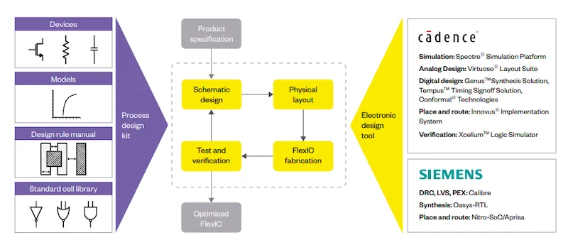
FlexIC process design kit.
To manage signal routing across larger circuit designs, the platform uses four metal layers with a 4-µm routing pitch. Packaging integrates a 5.5-µm passivation layer and a 1.5-µm aluminum redistribution layer (RDL) to support electrical interfacing through flexible or hybrid methods. The total thickness of the fabricated FlexICs reaches approximately 37 µm, with a bend radius of 5 mm.
To support design and deployment, the platform includes a process design kit (PDK) compatible with Cadence and Siemens EDA tools.
Redefining NFC’s Role in Everyday Interactions
As global supply chains seek scalable ways to embed digital intelligence into disposable and semi-disposable goods, flexible NFC solutions like the PR1301 can bring new dynamics into the discussion. As of now, volume samples of the PR1301 are available through Pragmatic’s distribution channels, with options for singulated dies, frame-mounted wafers, and sample inlays.

EA-CHIP INDUSTRY CO., LIMITED
-
Tel
+86 180 2549 2789 -
Wechat