BOM
BOM Cart()
 English
 Russia
 Korean
Recent research breakthroughs are pushing semiconductors far beyond traditional logic and memory roles into chemical catalysis, sustainable manufacturing, and quantum photonics.
The last few decades of semiconductor progress have focused on shrinking transistors and packing more compute into less space.
But a new wave of research is expanding what semiconductors can do, not just how small or fast they are. In labs across Tokyo, Virginia, and Germany, engineers are rethinking these materials as programmable catalysts, eco-friendly nanostructures, and light-emitting quantum layers.
Semiconductors Show Promise for Efficient Carbon Capture
In a bid to tackle the inefficiencies of current carbon dioxide utilization technologies, researchers at the Institute of Science Tokyo have turned to an unlikely candidate for catalytic chemistry: semiconductors.
Their work centers on a class of amorphous indium-gallium-zinc oxide (a-IGZO) materials, better known for their role in display technology, that can be tuned electronically to drive selective CO₂-to-methanol conversions. The team’s palladium-loaded version of this semiconductor catalyst achieved a remarkable 91% selectivity for methanol, outpacing conventional copper-zinc oxide systems that often generate excessive carbon monoxide as a byproduct.
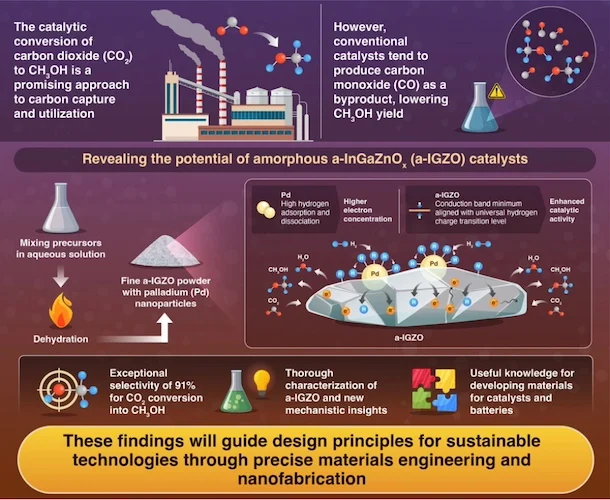
An infographic depicting carbon dioxide’s conversion to methanol by hydrogen species on n-type oxide semiconductors. Image used courtesy of the Journal of the American Chemical Society
Rather than relying solely on traditional surface-bound catalytic activity, the researchers engineered the electronic band structure of a-IGZO to align with the so-called universal hydrogen charge transition level (UHCTL), enabling the simultaneous stabilization of both H⁺ and H⁻ species. This alignment allows the catalyst to facilitate all stages of the multi-step hydrogenation process necessary to transform CO₂ into methanol.
Palladium nanoparticles play a complementary role by dissociating molecular hydrogen and injecting reactive hydrogen atoms onto the oxide surface, where a high carrier concentration further enables efficient charge transfer across the Pd/semiconductor interface.
This work could lead to a shift in catalytic design, from focusing on reaction sites alone to orchestrating complex electron and ion interactions within the material itself. Beyond high selectivity, the method also suggests new guidelines for engineering electronic materials with catalytic potential, with implications for chemical production, energy storage, and carbon-neutral fuel synthesis.
New Semiconductor for Future Computer Chips
In pursuit of a silicon-compatible semiconductor capable of bridging electronics, photonics, and quantum technologies, researchers at Forschungszentrum Jülich and the Leibniz Institute for Innovative Microelectronics have developed an alloy of carbon, silicon, germanium, and tin, which represents an unprecedented combination within Group IV.
Dubbed CSiGeSn, this material overcomes long-standing chemical incompatibilities (such as the disparity between carbon's and tin's atomic radii) by refining epitaxial growth conditions using off-the-shelf chemical vapor deposition (CVD) systems. The result is a structurally stable, compositionally uniform crystal lattice that remains compatible with existing CMOS manufacturing.
Dr. Dan Buca (left) and Andreas Tiedemann (right) at the CVD system from Aixtron, used for coating the wafer. Image used courtesy of Forschungszentrum Jülich
The unique blend enables bandgap tuning beyond what’s possible with traditional Group IV semiconductors alone, opening up new device behaviors at room temperature—particularly in optoelectronics.
Early demonstrations include the first quantum-well light-emitting diode (LED) fabricated from this quartet, offering a proof of concept for integrated lasers, photodetectors, and thermoelectric devices directly on silicon wafers. Because it maintains lattice continuity while adding new electronic and photonic degrees of freedom, the alloy could lay the groundwork for scalable on-chip quantum and photonic computing, energy-harvesting systems, and advanced wearables.
An Eco-Friendly Method for Creating Semiconductor Materials
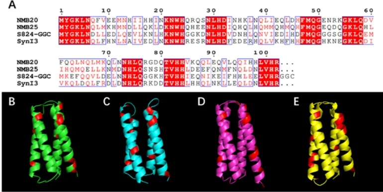
To address the environmental toll of semiconductor manufacturing, especially the reliance on toxic solvents and high-temperature processes, researchers at Virginia Commonwealth University have demonstrated a green method for synthesizing semiconductor quantum dots using engineered proteins.
Rather than refining rare earth metals or processing heavy metals through conventional chemical routes, this approach mimics biological mineralization, leveraging de novo protein design to control the nucleation and growth of functional nanomaterials in aqueous environments at room temperature.

De novo protein-based quantum dot capping agents. (A) Sequences of four de novo proteins employed as capping agents. Conserved residues from the design are highlighted in red, while regions containing different residues with shared polarity or nonpolarity are shown in black and red font (B-E). Image used courtesy of ACS Central Science
Unlike naturally occurring biomineralization processes, which are limited by the properties of evolved proteins, the team’s use of synthetic, purpose-built proteins enables precise control over material characteristics, including particle size, shape, and composition. This breakthrough allows quantum dot formation without high heat, pressure, or hazardous byproducts, greatly lowering both environmental impact and energy cost. Early results suggest the method is scalable and compatible with tunable bandgap engineering, making it applicable to optoelectronics, sensors, and bio-integrated devices.
Beyond its immediate ecological benefits, the work opens a new frontier in materials science where protein engineering intersects with semiconductor fabrication. With support from DARPA and broader interest in sustainable tech, this line of research could lead to a new class of cleanroom-free, bio-fabricated electronic components.

EA-CHIP INDUSTRY CO., LIMITED
-
Tel
+86 180 2549 2789 -
Wechat