Toshiba’s SOP Advance(E) package yields lower losses and better thermal performance.
Toshiba has introduced two N-channel power MOSFETs featuring the company’s latest packaging technology, SOP Advance(E). Targeted for high-performance switched-mode power supplies in industrial sectors, the devices aim to unlock lower loss, higher efficiency, and decreased thermal strain for data centers and telecommunications alike.
Toshiba’s new power MOSFETs. Image used courtesyof Toshiba
The MOSFET Devices’ Tech
The two devices, the PM1R908QM and TPM7R10CQ5, are both newsworthy for a handful of reasons.
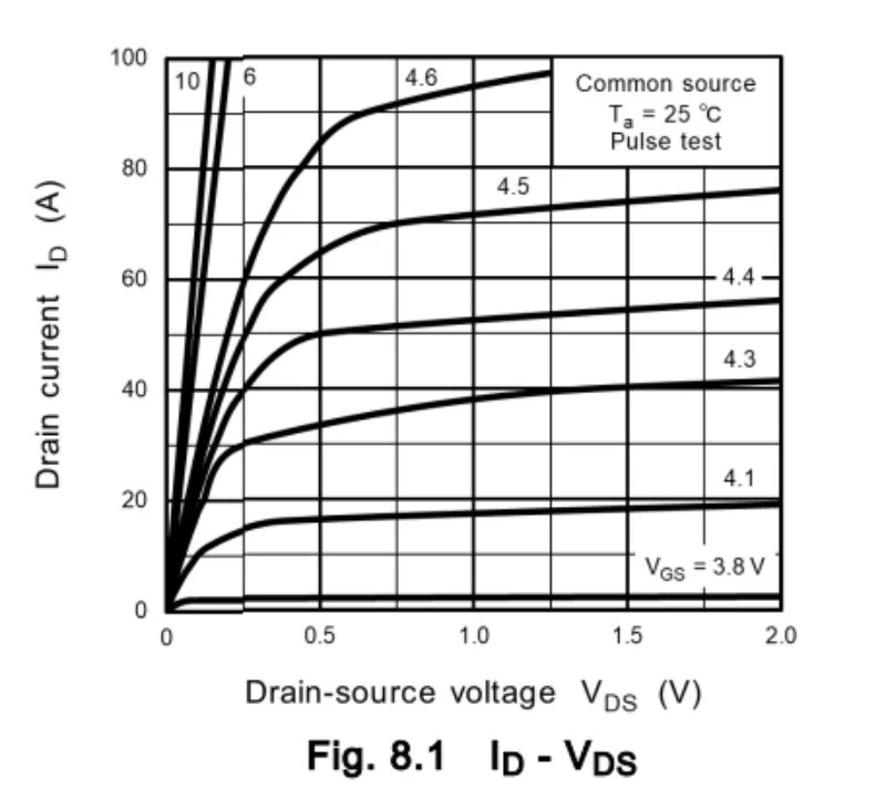
The TPM1R908QM is an 80 V-rated power MOSFET with a typical drain-source on-resistance (RDS(on)) of 1.5 mΩ and a maximum of 1.9 mΩ at VGS = 10 V. It supports a drain current of up to 238 A at a case temperature of 25°C and has a dynamic performance bolstered by a low gate-switching charge of 35 nC and an output charge of 111 nC for reduced switching losses. The total gate charge is 108 nC, and the device exhibits a fast switching profile with a typical rise time of 50 ns and fall time of 38 ns. A channel-to-case resistance of just 0.6°C/W optimizes its thermal performance.
The TPM1R908QM’s output characteristic curve. Image used courtesy of Toshiba
The TPM7R10CQ5 is rated at 150 V and offers a maximum RDS(on) of 7.1 mΩ (typical 5.7 mΩ) at VGS = 10 V. It can sustain a drain current of 120 A at 25°C case temperature. Switching characteristics include a fast reverse recovery time of 45 ns and a low reverse recovery charge of 43 nC. The gate-switching charge is 18 nC, while the output charge is 106 nC. Together, these specifications could enable better performance in synchronous rectification applications.
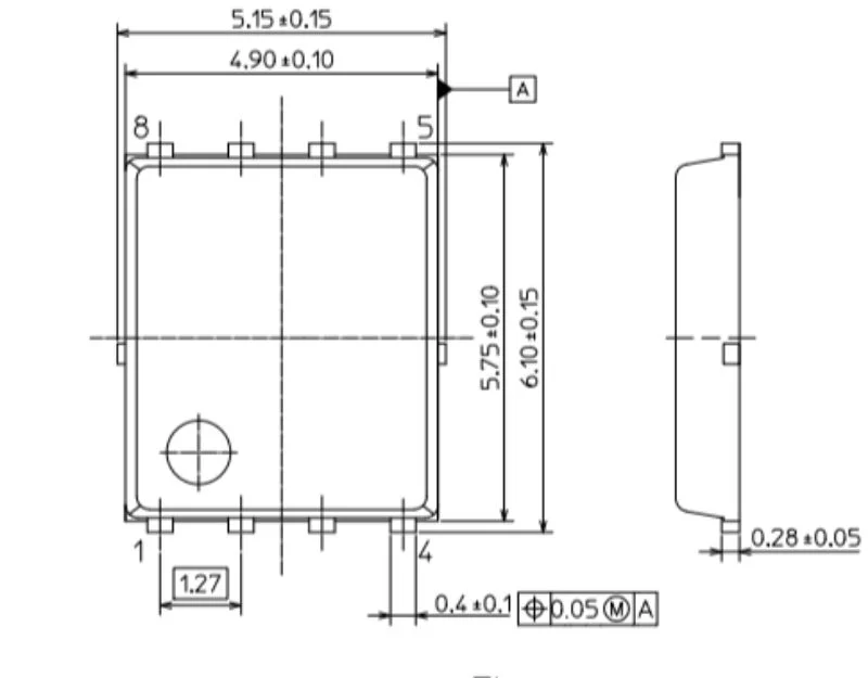
Both devices come in the same compact SOP Advance(E) package footprint of 4.9 mm × 6.1 mm.
SOP Advance(E)
While semiconductor parameters influence power MOSFET efficiency, packaging is also a major contributor. In applications with high switching frequencies and current densities, electrical and thermal parasitics introduced by traditional packages can bottleneck performance and increase power losses.
The SOP Advance(E) format addresses these challenges with a redesigned internal layout that minimizes lead inductance and improves thermal conduction paths. According to Toshiba, the result is a significant 65% and 15% reduction in package resistance and thermal resistance compared to the earlier SOP Advance(N) design, respectively. The drop in package resistance directly reduces conduction losses, while the decrease in thermal resistance delays thermal saturation under load.
Packaging dimensions for the SOP Advance(E). Image used courtesy of Toshiba
Because of these advancements, the TPM1R908QM and TPM7R10CQ5 can operate at a maximum channel temperature of 175°C.
Efficiency Gains for Industrial Power Systems
With advances in semiconductor and packaging technology leading to significant gains in performance and efficiency, Toshiba’s TPM1R908QM and TPM7R10CQ5 may be a good option for modern industrial and infrastructure applications. Both MOSFETs are currently in commercial production and available through authorized distributors. They also include support for Toshiba’s G0 and G2 SPICE models, which support fast and accurate simulation during circuit design.
-
Tel
+86 180 2549 2789 -
Wechat

 BOM
BOM Cart()
 English
 Russia
 Korean


