BOM
BOM Cart()
 English
 Russia
 Korean
In 1970, Intel’s 1103 became the first commercially successful DRAM chip, and the first time a semiconductor memory beat magnetic core at its own game: price, density, and logic-level compatibility.
In the early 1970s, most digital systems still used magnetic core memory—dense meshes of hand-wired ferrite rings. It worked, but it was bulky, expensive, and labor-intensive to manufacture. If semiconductor memory was ever going to replace it, it had to match core memory’s performance and beat it on cost.
That’s exactly what the Intel 1103, released in October 1970, set out to do. Developed in collaboration with Bill Regitz and Bob Proebsting from Honeywell, the 1103 was based on a three-transistor (3T) dynamic cell design that traded off complexity and area for manufacturability. At just $60 at launch (or roughly one cent per bit), it was significantly cheaper than core memory. As yields improved, the cost dropped to ~$4 per chip by 1973.
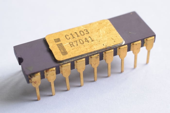
A ceramic Intel 1103 variant, the C1103. Image (modified) used courtesy of Thomas Nguyen via Wikimedia Commons (CC BY-SA 4.0)
Despite a rough start, the 1103 became the first widely used semiconductor DRAM, and the first to seriously challenge magnetic core in both technical and commercial viability. By 1971, it was the best-selling semiconductor memory chip in the world. Within two years, 14 of the 18 major computer manufacturers—including HP, DEC, Honeywell, and CDC—had adopted it.
Its performance wasn’t exceptional, but it was fast enough for many logic-level applications, especially in mini- and mainframe systems. Designers didn’t love it, but they used it because it made economic sense.
Inside the 1103
Technically, the 1103 was modest, even by 1970 standards. It packed 1,024 bits (1024 x 1) into an 18-pin dual in-line package, built using a p-MOS 8-μm, silicon-gate process. At the heart of each bit was a three-transistor dynamic memory cell: simple, compact, and fast enough when supported with good-sense amplifiers.
Internally, the memory was arranged as a 32 x 32 bit array. The chip used 32-sense amplifiers to read or refresh one full row at a time. To refresh the entire memory, the system needed to access all 32 rows every two milliseconds. In practice, many designers implemented burst refresh strategies, often reading a full array at once to reset all dynamic cells within the window.
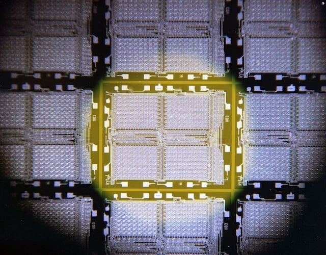
DRAM memory cell of the Intel 1103. Image used courtesy of Chrihern via Wikimedia Commons (CC BY-SA 3.0)
The I/O was not TTL-compatible in its original form. The 1103 used higher voltage levels (~16 V) and was finicky about clock timing, chip enable overlaps, and setup/hold margins. That meant adding refresh logic externally, an overhead that required careful controller design, but that was still simpler than managing magnetic core memory’s read-destructive operations and massive physical footprint.
These quirks made it difficult to integrate with standard logic without additional buffers or interface circuitry. Still, the logic compatibility, scalability, and manufacturability gave it an edge over magnetic core and made it one of the first truly viable DRAMs for system memory.
The Chip Designers Loved to Hate
Early adopters of the 1103 found it frustrating. Its timing diagrams were unforgiving. Setup and hold margins were narrow. The refresh requirement was strict, and the control signals had to be well-behaved to avoid data corruption. As Intel’s sales manager A. C. “Mike” Markkula put it in 1973, “They hate it, but they use it,” summing up the 1103’s rough edges, but undeniable appeal.
Intel’s initial silicon also suffered from yield issues, forcing multiple mask revisions, or “steppings,” before the chip stabilized in high volume. According to later retrospectives, it wasn’t until the fifth mask version that 1103 chips could be shipped reliably at scale. To ease integration pain, Intel followed up with the 1103A, which introduced improved timing margins, on-chip address buffers, lower power draw, and TTL-compatible inputs and outputs.
Intel calls the 1103 the “death knell for magnetic core memory's dominance.” Image used courtesy of Intel
The 1103A became a drop-in replacement, dramatically simplifying memory controller design and improving adoption rates. With the bugs ironed out, system vendors flocked to it. Systems like HP’s 9800 series, DEC’s PDP-11, and various Honeywell minis adopted the 1103/1103A for main memory. Intel quickly spun out a family of support ICs to reduce integration effort further.
By 1973, it was clear that core memory was on the way out and semiconductor DRAM was here to stay.
Laying the Groundwork for DRAM
Ultimately, the Intel 1103 proved that semiconductor memory could scale not just in density but also in volume, affordability, and compatibility.
While the 1103 used 3T dynamic cells and p-MOS technology, it laid the groundwork for the single-transistor DRAM cells that followed (such as the Intel 2104 and the 4-Kb, n-MOS chips of the mid-1970s). It also defined a pattern that DRAM continues to follow to this day.
If you’re designing memory systems today, the 1103 is a reminder that the most disruptive designs aren’t always the most elegant, and that system-level economics often matter more than perfection at the transistor level.
Were you one of the first designers who “loved to hate” the Intel 1103 when it made its debut? Tell us about your experience with it—or any other legacy technology—in the comments below.

EA-CHIP INDUSTRY CO., LIMITED
-
Tel
+86 180 2549 2789 -
Wechat