BOM
BOM Cart()
 English
 Russia
 Korean
The vertical GaN (vGaN) power semiconductors claim to boost performance and efficiency in data centers, EVs, and renewables.
Onsemi has launched its vertical gallium nitride (vGaN) power semiconductor family, a next-generation GaN-on-GaN technology for the energy and performance demands of artificial intelligence, electric vehicles, and renewables.
Learn more about Onsemi’s vertical GaN technology. Video used courtesy of Onsemi
Developed at the company’s 66,000-square-foot facility in Syracuse, New York, these devices are the first commercially scalable implementation of true GaN-on-GaN power architecture, according to Onsemi.
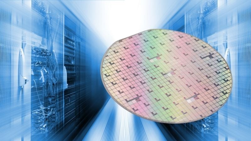
The vertical GaN wafer. Image used courtesy of Onsemi
Vertical GaN Architecture and Performance
Onsemi’s vertical GaN transistors are fabricated on bulk GaN substrates, which allow current to flow vertically through the crystal lattice rather than laterally across its surface. This approach is the differentiator in device performance.
Since vertical GaN eliminates the substrate mismatch inherent to GaN-on-silicon or GaN-on-sapphire processes, it reaches defect densities as low as 10^3–10^5 cm^-2, compared to ~10^9 cm^-2 for GaN-on-Si. As a result, it offers improved yield, dislocation rates, and ruggedness.
To manufacture vertical GaN, Onsemi had to epitaxially grow thick, defect-free GaN layers at temperatures above 1,000°C. In-situ doping formed p- and n-type regions. The company boasts over 130 patents covering growth, regrowth, and device fabrication techniques, including unique processes for regrowing p-GaN on patterned wafers.
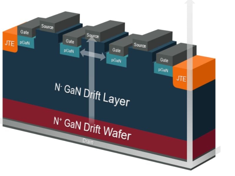
Vertical GaN device structure. Image used courtesy of Onsemi
The devices leverage a hexagonal wurtzite crystal structure, which offers a 3.4 eV bandgap and critical electric field strength of 3.3 MV/cm. The structure also supports high electron mobility (~ 2,000 cm^2/V·s) and peak electron velocity near 2.5×10^7 cm/s to unlock switching frequencies well beyond those achievable with Si or SiC MOSFETs.
According to the reported performance metrics, vertical GaN devices can handle voltages of 1,200 V and above, with prototypes demonstrating up to 3,300 V. Systems based on vGaN are also reported to reduce power-conversion losses by up to 50%. The device’s higher switching frequencies unlock proportional reductions in the size of inductors, capacitors, and magnetic components. Compared to lateral GaN, vGaN devices occupy roughly one-third the area.
GaN-on-GaN Power Semiconductors
In conventional lateral GaN devices, the GaN layer sits atop a foreign substrate such as silicon. This arrangement introduces lattice and thermal mismatches that limit thickness and voltage capability.
In contrast, GaN-on-GaN, or homoepitaxial GaN, grows the active region directly on a native GaN substrate. The absence of lattice strain allows engineers to build much thicker drift regions, increasing breakdown voltages well past 1 kV while maintaining low on-resistance. Meanwhile, the vertical current path reduces electric-field crowding at the surface and enhances avalanche ruggedness.
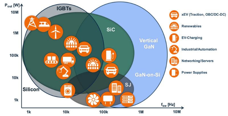
Power versus switching frequency for various power technologies. Image used courtesy of Onsemi
GaN’s wide bandgap (3.4 eV) and high electron mobility produce a Baliga figure of merit nearly 10,000 times that of silicon, translating into lower conduction losses and higher switching efficiency. When operated at high frequency, converters can use smaller passive elements, which directly reduces the overall system size and cost. Additionally, GaN’s thermal conductivity and low defect density offer improved high-temperature operation.
Still, challenges remain in cost and wafer availability. Producing bulk GaN substrates is more complex and expensive than silicon, as it requires high-temperature, high-pressure crystal growth. Yet, as fabrication scales and yields improve, vertical GaN could one day displace lateral GaN and even SiC in applications that demand both high voltage and compact form factors.
Toward Scalable High-Density Power
Onsemi reports that sampling of 700 V and 1,200 V vGaN devices is underway, with full production expected to follow once qualification is complete.

EA-CHIP INDUSTRY CO., LIMITED
-
Tel
+86 180 2549 2789 -
Wechat