BOM
BOM Cart()
 English
 Russia
 Korean
The company optimized the device's dual-voltage design for high-speed, low-power 1.2 V SoC applications.
System designers working at the intersection of performance and extreme power efficiency have had limited options for external NOR flash. Traditional 1.8 V devices deliver stability but require extra level shifting when paired with modern 1.2 V SoCs. Lower-voltage flash exists, but it often sacrifices speed or robustness. Gigadevice aims to close that gap with its newly launched GD25NX series, an xSPI NOR flash line built on a dual-voltage architecture explicitly designed for 1.2 V digital platforms.

Gigadevice’s new GD25NX dual-voltage xSPI NOR flash series for next-generation 1.2 V SoCs.
With a 1.8 V core and native 1.2 V I/O, the GD25NX connects directly to low-voltage SoCs without an external booster. That single design choice does more than trim a few components off a board. It reshapes the power and performance profile of wearables, automotive controllers, edge AI modules, and data-center hardware where every milliwatt and microsecond matter.
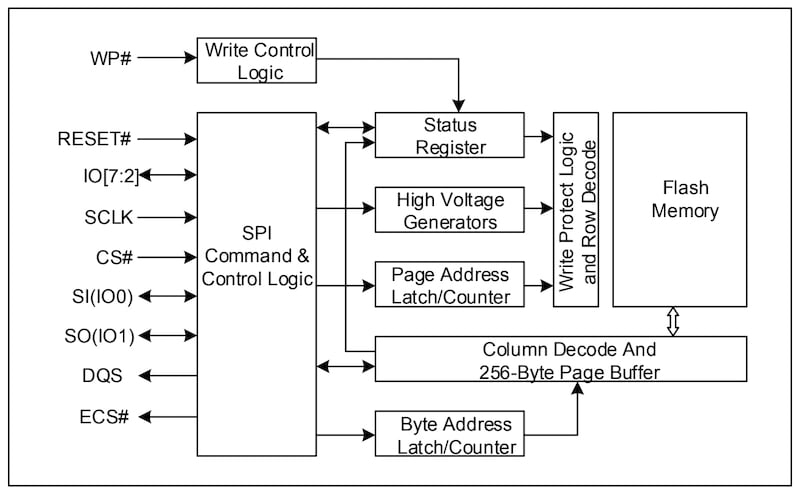
The flagship 128 Mbit device (GD25NX128J) is part of Gigadevice’s uniform-sector, xSPI-enabled flash family, supporting both standard SPI and high-bandwidth octal modes with single transfer rate (STR) and double transfer rate (DTR) operation.
What Sets the GD25NX Series Apart
Although it inherits some lineage from Gigadevice’s earlier GD25NF and GD25NE lines, the GD25NX is not just an incremental voltage tweak. Its architecture introduces several distinguishing features that directly target the needs of next-generation SoCs.
The most critical is the dual-voltage interface. Many advanced chipsets, especially in AI-enabled wearables and modern MCUs, operate at 1.2 V on the I/O level. The GD25NX’s ability to run its I/O at the same voltage eliminates the need for voltage-boosting hardware, reducing system power consumption and simplifying board design. This isn’t theoretical; the series’ read current at 200 MHz measures just 16 mA in octal STR mode and 24 mA in octal DTR mode, representing up to a 50% reduction in read power versus older 1.8 V octal flash products.
Internal block diagram of the GD25NX series showing DQS timing support, ECC hardware, page buffers, and the high-speed octal SPI architecture.
The device also leans hard into xSPI performance, supporting octal SPI with speeds up to 200 MHz across STR and DTR. In DTR mode, where data transfers occur on both clock edges, the throughput reaches 400 MB/s, rivaling the bandwidth historically reserved for broader parallel interfaces. Page program time sits at 0.12 ms, while sector erase completes in 27 ms, yielding a 30% improvement in write performance over previous 1.8 V designs. To maintain speed at these frequencies, Gigadevice integrates a data-strobe (DQS) signal for timing alignment and offers a “pre-drive” feature that begins output activation one clock early to stabilize high-speed reads.
Reliability also gets hardware attention. The GD25NX line includes built-in single-error correction and double-error detection (ECC) for every aligned 16-byte chunk, as well as CRC checking to validate high-speed DTR transfers. The ECS# pin provides error-indicator output, a real-time hardware signal that pulls low if a correction occurs during a read burst. The combination gives the flash a deeper safety net in noisy environments, such as automotive ECUs and server-class AI accelerators.
Performance Metrics That Change System Behavior
Raw speed is one thing; meaningful system-level behavior changes are another. Gigadevice says the GD25NX series delivers both.
At 200 MHz octal I/O, the flash can sustain throughput that supports execute-in-place (XiP) workloads in real time. This is particularly important for AI-centric SoCs that fetch instruction streams or model parameters directly from external memory. The GD25NX’s low latency and optional continuous-read mode minimize instruction stalls, while its wrap-around burst modes (16, 32, or 64 bytes) align cleanly with standard cache-line sizes, reducing command overhead.
Power consumption is the second pillar. By operating natively at 1.2 V, the flash avoids wasting energy through level shifting. The datasheet’s DC characteristics show read currents at 166–200 MHz that are less than half those of 1.8 V NOR flash under the same conditions. For battery-constrained platforms, that translates into longer operating life without slowing the memory interface.
Erase and program metrics follow suit. The 27 ms sector erase and 0.12 ms page program times put the GD25NX among the fastest NOR options in its class. Faster erase and write cycles enable more responsive firmware updates, quicker data logging, and improved runtime patching, a key for IoT devices that need continuous over-the-air updates.
Where the GD25NX Series Fits
Gigadevice positions the GD25NX for four major sectors: wearables, edge AI, data centers, and automotive electronics. Each gains something different from the low-voltage, high-bandwidth design.
Wearables benefit most from the efficiency profile. A 1.2 V I/O flash cuts both active and standby power draw and drops the BOM cost by removing level shifters. Small packages such as the TFBGA-24 (5×5 array) and compact WLCSP fit directly into dense wrist-mounted PCBs.
Edge AI modules benefit from the 400 MB/s DTR throughput, which is sufficient to stream neural network weights directly from NOR flash for inference workloads. Many edge SoCs use NOR flash for model storage because it offers deterministic read latencies; the GD25NX simply raises the performance ceiling while retaining that predictability.
Data-center appliances, especially smart-NICs, controllers, and accelerator boards, benefit from stability features such as ECC, CRC, the DQS timing signal, continuous-read support, and wrap-based data patterns that align with modern caching architectures. These systems often operate in electrically noisy environments, making the error-monitoring ECS# pin a real asset.
Automotive electronics leverage both error-correction hardware and high-temperature support. The GD25NX128J, for example, is available in versions rated up to -40°C to 125°C, aligning with automotive-grade qualification ranges listed in the ordering information table. The fast erase and program speeds reduce ECU reflash times and improve OTA update reliability, which is essential as vehicles adopt increasingly software-defined architectures.
A Platform Built for Next-Generation SoCs
The GD25NX series is not just a voltage-optimized NOR flash. It’s a response to the radical changes in SoC design over the last decade. Low-voltage interfaces, data-intensive workloads, and the need for faster boot and fetch cycles require an external memory subsystem that can keep up without consuming excessive power. By delivering 1.2 V native I/O, 200-MHz octal operation, 400 MB/s DTR throughput, built-in ECC/CRC, and improved erase/write speeds—all in a compact package, Gigadevice is offering a flash architecture built around the real constraints of modern hardware.
Samples of the GD25NX128J (128 Mb) are already available, with the 64-MB GD25NX64J following shortly. Broader densities and packages are planned as the company expands the portfolio.
All images used courtesy of Gigadevice.

EA-CHIP INDUSTRY CO., LIMITED
-
Tel
+86 180 2549 2789 -
Wechat