BOM
BOM Cart()
 English
 Russia
 Korean
OpenAI and Broadcom sent shockwaves through the industry by announcing Jalapeño, OpenAI's first custom AI accelerator.
OpenAI is widely accepted as the pioneer in modern AI development, with its 2022 ChatGPT launch kicking off the modern AI race as we know it. Up to this point, the company has run its models and services primarily on Nvidia's GPUs. However, running its models on hardware it neither designs nor controls has made serving frontier models at scale costly and almost prohibitive.

OpenAI CEO Sam Altman and Broadcom CEO Hock Tan holding Jalapeño. Image used courtesy of OpenAI
By designing its own silicon, OpenAI gains direct control over the performance, cost, and efficiency of the infrastructure behind ChatGPT, Codex, and its API, and reduces its reliance on third-party compute suppliers. Jalapeño is the first accelerator in a multi-generation platform OpenAI and Broadcom are building together, with Celestica contributing board, rack, and system integration expertise.
Detailing Jalapeño
While many technical specifications and benchmarks are not available, OpenAI claims Jalapeño will resolve the workload-to-hardware mismatch that many companies face when serving frontier AI models at scale.
While GPUs offer massive parallelism and are a great solution for AI training, they face notorious underutilization during AI inference. As a result, GPUs waste significant power, die area, and CapEx in the datacenter, all of which impact cost per token and user adoption. As OpenAI has developed larger models, this cost-to-performance gap has reached a fever pitch. OpenAI realized it could not continue using hardware designed for someone else’s requirements.
The company led Jalapeño's architectural design, drawing on its daily observations of inference patterns across ChatGPT, Codex, and its API. Broadcom handled silicon implementation and contributed its Tomahawk networking silicon to bring the platform to large-scale production. Celestica provided board, rack, and system expertise to industrialize the design. Together, the three companies built Jalapeño from scratch on a 3-nm process, tailored to the specific memory movement, compute, and networking patterns of LLM inference.
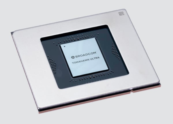
Broadcom's Tomahawk Ultra Ethernet switch series. Image used courtesy of Broadcom
The goal, according to OpenAI, is to combine the throughput of today's leading AI accelerators with latency levels closer to those of the fastest specialized inference systems. The company says engineering samples are already running ML workloads at production-target frequency and power, including GPT-5.3-Codex-Spark. Early testing indicates the chip will deliver substantially better performance per watt than competing accelerators.
Why LLM Inference Calls for Purpose-Built Silicon
Compared to ASICs, GPUs are general-purpose computing resources, used for tasks ranging from 3D rendering to scientific simulation. As such, when a GPU handles LLM inference, it routes data through compute and memory hierarchies designed for a broader class of tasks, ultimately wasting power and die area.
In contrast to GPUs’ general-purpose architecture, LLM inference, like many workloads, follows a narrow set of computational patterns. Typically, inference consists of large matrix multiplications over weight tensors, attention computations across token sequences, and autoregressive token generation one step at a time. Each pattern creates predictable bottlenecks around memory bandwidth, inter-chip communication, and hardware sustainability near theoretical peak throughput.
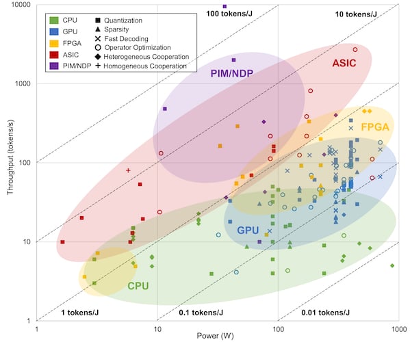
A comparison of the power and throughput of different hardware platforms when running AI inference. Image used courtesy of ArXiv
OpenAI designed an ASIC to address those bottlenecks by trading flexibility for efficiency. ASIC designers commit to fine-tune their silicon architecture to serve a specific workload, allocating die area, memory bandwidth, and power budget precisely according to what the task requires. No resources sit idle.
For LLM inference specifically, on-chip memory capacity and bandwidth must keep weight matrices and activations close to the compute. High-speed inter-chip interconnects coordinate across multiple accelerators serving a single model, and the networking fabric must scale across racks without creating communication bottlenecks. When engineers tune an architecture to transformer inference profiles, utilization climbs because the design carries no die area or power budget for features the task never uses.
A Nine-Month Development Cycle and a Multi-Generation Platform
According to OpenAI, the companies moved the chip from initial design to manufacturing tape-out in nine months, which they describe as the fastest ASIC development cycle ever achieved in semiconductor development. OpenAI attributes that pace to deep software-hardware co-development with Broadcom and to its own AI models, which accelerated the design process. Greg Brockman, OpenAI’s president, told CNBC that the degree to which its models compressed the timeline “was very surprising to us.”
Jalapeño is the first step in a multi-generation compute platform that OpenAI and Broadcom plan to deploy at a gigawatt scale with data center partners. The companies are targeting initial deployment by the end of 2026, with Broadcom CEO Hock Tan describing the late-2026 period as “small prototype development.” Full production will ramp up in 2027, and “full tilt” output will proceed in the first half of 2028.

EA-CHIP INDUSTRY CO., LIMITED
-
Tel
+86 180 2549 2789 -
Wechat